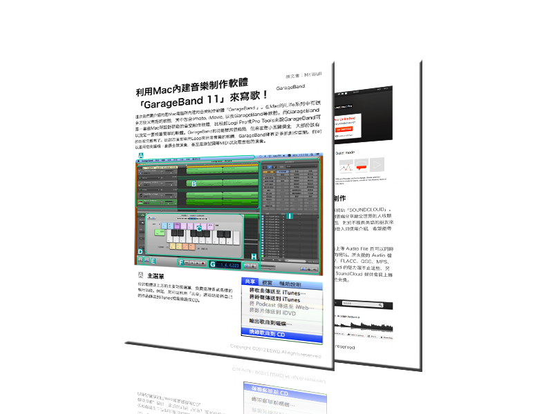
訂閱免費電子雜誌
現在只需填寫下面的表格並點擊【開始訂閱】,你就可以免費獲得【Garageband 操作解析】、【SOUNDCLOUD 登錄功能解析】、【DTM 專門用語】.. 等免費電子書唷。
Improper RPMB cleaning or flashing corrupt files can make the eMMC chip permanently unbootable.
In the KMGD scheme, each test point has a designated role:
A designated soldering or bridging point used to force the chip into a specific, usually low-level, communication mode (like ISP—In-System Programming or EDL—Emergency Download Mode). kmgd test point
: The first step is identifying the KMGD test point on the circuit board. This usually involves referring to the device's technical manual or schematic diagram.
: In digital forensics, test points enable the extraction of data directly from the NAND flash, bypassing lock screens or encryption that would otherwise block access. Improper RPMB cleaning or flashing corrupt files can
The use of a KMGD test point can vary depending on the specific device or system it's associated with. However, the general process involves:
Test points generally range from 0.8 mm to 1.0 mm (32 to 40 mils) in diameter. This usually involves referring to the device's technical
Carefully open the smartphone casing. Disconnect the battery terminal completely. Working on a live circuit board increases the risk of shorting a high-voltage power line (like VCC or VCCQ) directly to a low-voltage data line, which will instantly kill the processor. Step 2: Locate the KMGD Test Point
Click or Flash . The software will communicate directly through the MROM/EDL state, bypassing the broken KMGD eMMC internal software structure to overwrite the corrupt boot partitions.
The KMGD chip is a highly compact, multi-chip package (eMCP) manufactured primarily by Samsung. It combines two critical components into a single BGA-221 ball configuration package:
Test points are rarely explicitly labeled as "KMGD" on a smartphone or tablet circuit board. Instead, they are small, exposed gold copper pads on the motherboard surface. Use these steps to locate the exact point: 1. Board Diagrams and Schematics
現在只需填寫下面的表格並點擊【開始訂閱】,你就可以免費獲得【Garageband 操作解析】、【SOUNDCLOUD 登錄功能解析】、【DTM 專門用語】.. 等免費電子書唷。